Editorial Team
Published on 7 May 2021


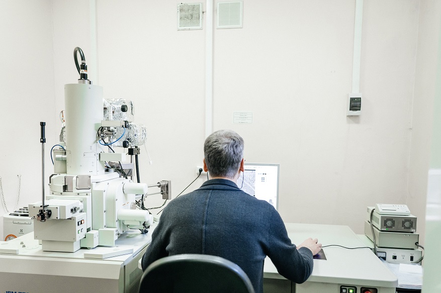
An ultra-high-resolution scanning electron microscope that is a part of the TPU Center for Collective Use, has been upgraded at the university. Using the microscope, it is possible to research the morphology and composition of structural elements of a wide variety of materials with resolution up to 1 nm. The renewal allowed reducing the research timing and increasing the quality of research findings.
The scanning electron microscope operates at TPU academic building No.10. The entire renewal conducted by the grant of the Ministry of Education and Science of the Russian Federation has already been finished.
“In 2008, a microscope of Japanese manufacturing was purchased at TPU within the project of the Federal Target Program for Development of Nanoindustrial Facilities, however, it has remained the only equipment at TPU allowing to research problematic samples of nanostructural materials with nanoscale resolution.
"It is implemented due to two features: the unsurpassed homogeneity of a cathode ray and the capability of operation at extremely low acceleration voltages. The closest tool with the same parameters from the same producer is located in Moscow, while alternative models with similar characteristics are not already produced by this producer or its rivals,” Edgar Dvilis, Senior Research Fellow of the TPU Innovation Center for Nanomaterials and Nanotechnologies, says.
The microscope allows scientists to see what structural elements are present in the materials they create, how they are distributed on the surface and related to it and each other. Using the microscope, nanoporous ceramics and membranes, nanoparticles, nanofibers and nanotubes, nanocrystals in the coating films are studied at TPU. Moreover, simultaneously with morphological analysis of the material, elemental analysis can be conducted to find out what chemical elements form the material.
A focused electron flux interacts with the material during the analysis. The products of this interaction are secondary electrons or back-scattered electrons, which are captured by special sensors from every particular point of the sample surface when it is scanned by the thinnest electron flux. Based on it, a complete picture of the material surface is formed in the fixed area.
“During the renewal, a more modern vacuum system was equipped at the microscope that allows preparing the tool for operation faster thereby significantly reducing overall analysis time. The microscope was equipped with an infrared video camera as well. Using this camera, an operator can observe what happens in a sample chamber and does not manipulate the samples randomly having no impact on the analysis results.
"Furthermore, a sputter cleaning installation was purchased to clean the sample surface from carbon contamination essentially affecting the analysis results. The sputter cleaning installation is multipurpose as it is designed for sample preparation not only of a scanning electron microscope but also for sample preparation of an ultra-high resolution transmission electron microscope that is one more unique installation possessed by TPU,” Edgar Dvilis explains.
It is planned that the renewal of the scanning electron microscope and transmission electron microscope will be continued in 2021. Particularly, for the scanning electron microscope, it is planned to purchase a modern product system of high-resolution energy dispersive X-ray analysis improving the quality of analysis results and not demanding resource-consuming liquid-nitrogen refrigeration.
The transmission electron microscope is planned to equip with a new high vacuum system and a set of improved sample holders for expanding a list of materials appropriate for analysis.