Published on 24 January 2021


In a recent study at Nagoya Institute of Technology, Japan, scientists have developed a novel non-destructive technique with enhanced depth resolution, which will bolster the development of efficient SiC devices for power generation and distribution systems. This new technique will help in the research and development of efficient high-voltage semiconducting devices for power systems.
Silicon carbide (SiC), a versatile and resistant material that exists in multiple crystalline forms, has attracted much attention thanks to its unique electronic properties. From its use in the first LED devices, to its applications in high-voltage devices with low power losses, SiC displays exceptional semiconductor behavior. So far, the operating voltages for unipolar SiC devices are below 3.3 kV. Though useful for the electronic systems of cars, trains, and home appliances, unipolar SiC-based devices cannot be used in power generation and distribution systems, which operate at voltages above 10 kV.
Some researchers believe that the solution to this conundrum lies in bipolar SiC devices, which offer low on-resistance (and hence lower losses) through conductivity modulation. However, the conductivity modulation effect is tightly related to the lifetime of excited charge carriers in the semiconductor; longer carrier lifetimes in the thick voltage blocking layer of SiC devices lead to increased modulation. On the other hand, excessively long carrier lifetimes increase the switching losses, and this trade-off has to be appropriately balanced by accurately controlling the distribution of carrier lifetimes within the semiconductor.
Unfortunately, most available techniques for measuring the carrier lifetime distribution of a semiconductor are destructive; the sample has to be cut for its cross-section to be analyzed. This motivated a research team from Japan, led by Associate Professor Masashi Kato from Nagoya Institute of Technology, to focus on improving one of the two existing non-destructive methods: time-resolved free-carrier absorption with intersectional lights (IL-TRFCA). In their new study published in Review of Scientific Instruments, the researchers present some impactful changes made to this technique (which they had previously pioneered) along with some very promising results.
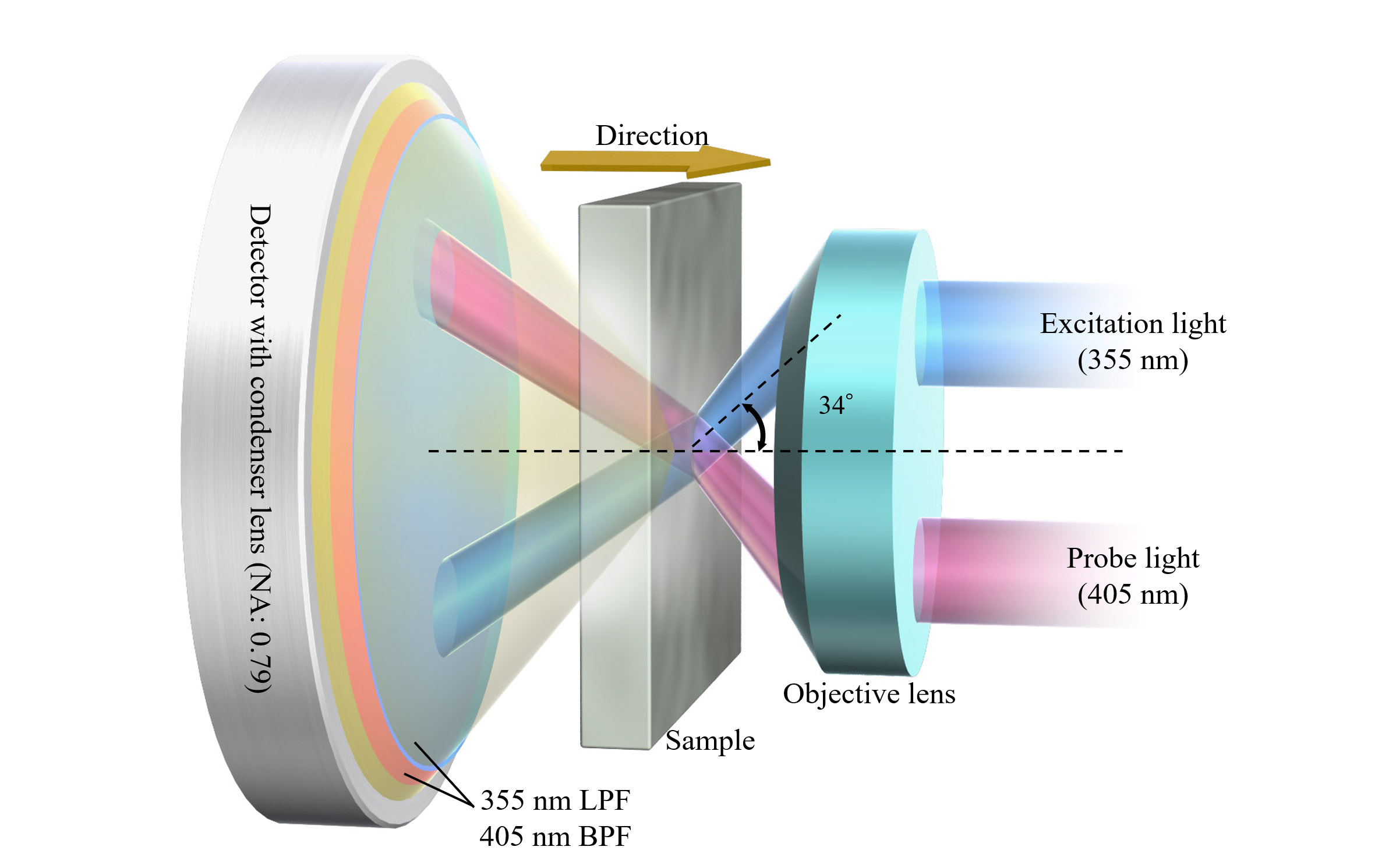
The IL-TRFCA method essentially consists of excitation laser, which creates photoexcited carriers and a probe laser plus a detector, which measure their lifetime. By pointing both lasers at the edges of an objective lens (see Figure 1), they are made to converge at the surface of the sample with opposite incidence angles. Then, the sample is moved towards the lens in micrometric steps, which causes the excitation and probe lasers to intersect not at the surface of the sample, but at progressively deeper regions. In this way, the scientists managed to measure the distribution of carrier lifetimes within the sample without the need to cut it.
Two substantial changes the researchers made to the IL-TRFCA method were the adoption of a larger incidence angle of 34° (34 degrees) for both lasers and a higher numerical aperture in the objective lens and detector. These modifications resulted in enhanced depth resolution and also made it possible to use IL-TRFCA in thicker SiC layers.
Excited about the results, Dr. Kato remarks, “Our non-destructive approach for measuring the distribution of carrier lifetimes allows one to determine the non-uniformity of a material without destroying the sample, which can then be used to fabricate devices, and research and develop bipolar SiC technology, such as high-voltage diodes and transistors.”
Having appropriate measurement techniques at one’s disposal is one of the most essential factors in materials research, and IL-TRFCA could easily pave the way for the study—and ultimately adoption—of SiC in ultrahigh-voltage applications.
In this regard, Dr. Kato comments, “SiC devices can operate with lower power consumption compared with conventional semiconductors, and their commercialization could result in a substantial reduction in energy consumption in power systems throughout the world. In turn, this could alleviate serious environmental threats such as the accumulation of greenhouse gases.”
Now that the tools have been laid out, it is time to delve deeper into how carrier lifetime distributions can be tuned in thick SiC and other semiconductors. Let us hope this leads us to more efficient devices and a more eco-friendly future!