Saint Petersburg Electrotechnical University
Published on 7 December 2021


A team of physicists from Saint Petersburg Electrotechnical University "LETI" studied and described the main factors that affect the transition of vanadium dioxide (VO2) thin films into the conducting state. The team identified two different transition mechanisms that depend on the number of defects in a sample: the fewer defects, the less voltage is required for transition, and the more independent voltage threshold is from temperature. The results of the study were published in the Chaos, Solitons & Fractals journal.
In their normal state, vanadium dioxide (VO2) films cannot conduct electricity. However, when subject to a certain voltage level, their resistance reduces by up to a hundred thousand times. Such a transition can happen very fast — in less than a picosecond. The mechanism of this process is still largely unknown, but this unique property makes vanadium dioxide films a promising material for smart windows, thermal imagery sensors, and artificial neurons for next-generation computers.
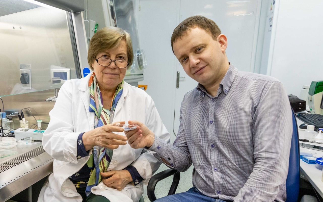
"One potential area of application of VO2 thin films is active memristors. Thanks to resistive switching in active memristors, they can be used to simulate the behavior of voltage-gated ion channels in biological neurons, and phase transition in VO2 thin films makes it possible to model different types of spike activity of neurons. Potentially, the modeling results could help scientists study the time synchronization of the neurons that support the functional activity of the brain and find ways for their synchronization or modulation. Based on these studies, non-pharmacological correction methods for certain functional brain states could be developed," says Natalia Andreeva, a lead researcher at the Nanotechnologies Science and Educational Center of ETU "LETI."
In its work, the team from ETU LETI studied the switching dynamics in a broad temperature range: from -200 to +20°С. To do so, they made several identical samples by covering a sapphire base with a thin layer of vanadium dioxide using the method of reactive magnetron sputtering. During this process, particles are dislodged from a bar of the sputtered material by gas ions in a strong magnetic field. Then, different voltage levels were applied to the samples at different temperatures, and the team studied the current flows through VO2 thin films.
Based on the experiment results, the team divided all VO2 thin film samples into two types. The first one required more voltage to transition to the conducting state when the temperatures went down, and the second one did not exhibit any threshold voltage changes correlating with temperature. According to the team, the difference might be due to the number of defects, namely, ions of hydrogen and oxygen vacancies (i.e. areas lacking atoms of oxygen).
In some cases, the defects could act as electron traps, and for the transition to the conducting state to happen, all of them should be filled. This requires a certain threshold voltage. When a sample has a relatively small number of defects, the threshold voltage is low and does not depend on the temperature; the transition to the low resistance state in VO2 thin films is preferably electronically driven. On the contrary, at increasing the number of defects in a sample, the higher voltage bias is required for the transition to the low resistance state, and more likely that it is triggered due to thermal heating. In this case, the threshold voltage is temperature-dependent. When a sample is cooled down and subject to a voltage at the same time, more voltage is required for the transition with the temperature decreasing.
"We are going to continue working on this task in the framework of the state project "Bionic neuroarchitectonics." Namely, we plan to model neuroprocessing activity using cutting-edge smart materials and technologies," concluded Natalia Andreeva.